
The Intel Innovation 2023 event is only a few hours away, and we eagerly await the launch of the latest 14th-Gen processors, codenamed Meteor Lake. While many of us will drone in on the architecture, graphics, clock speeds, and the nitty-gritty of these next-gen processors, do you ever stop to wonder how Intel makes its chips? What are the exact steps involved from start to end? Well, I didn’t know either, but recently, Intel gave me the opportunity to visit their factories in Malaysia, and it was quite a learning experience. So, let this be a window into what goes on behind the scenes in Intel’s chip manufacturing facilities.
Note: Thanks to Intel for inviting Beebom and sponsoring our trip to Penang, Malaysia, as part of Tech Tour 2023. We also thank Intel for opening the doors of their factories to us in August 2023.
Intel Malaysia: Kulim and Penang Facilities
Before we talk about the step-by-step manufacturing process, let me give you a quick brief about Intel Malaysia. The Penang facility was the company’s first off-shore site outside the US, set up back in 1972. It started with 100 employees but now spans two Intel facilities, one in Penang and the other in Kulim, and employs 15,000+ employees.
As part of Intel Tech Tour 2023, which was a two-day affair, we first visited the Penang facilities on Day 1, and then an hour-long bus ride took us to the Kulim plant on Day 2. These two facilities handle the manufacturing operations, from wafer slicing & testing to assembling Intel Core and Xeon processors, except for wafer fabrication. It is one of the most important cogs in a well-oiled machine, assembling the upcoming Meteor Lake chips that will be announced soon.


Though Penang was our first stop on the tour, it is the Kulim KM2 facility where an Intel chip begins its journey. This location carries out the Die Prep and Die Sort operation, which I’ve explained in detail below, and then the die is transported to the Penang facility, where the processor is brought to life – assembled, stress-tested, and made sure it’s ready for use.
Intel Kulim: Die Prep & Die Sort
A morning bus ride across the Penang bridge brought me and other global media personnel to the KMDSDP facility in Kulim. Here, we all donned protective gear and headed into the first laboratory, where the Die Preparation process happens.
Step 1: Die Preparation
Everyone was in awe when we entered, as the laboratory was bathed in amber (orange) lighting. Why? It’s because the silicon wafers are attached to a mylar sheet, which is sensitive to UV lightning and loses its stickiness pretty quickly. Thus, amber lighting is necessary for this part of the process, ensuring the dies stay in position when cut and separated.
Note: Here, we also learned that the 300mm silicon wafers used for making the die aren’t created at the Malaysian factories but are instead shipped from Intel’s fabs in the United States, Israel, and other locations.

After being attached to the mylar sheet, the silicon wafer goes through a multi-step process. Firstly, it might go through a grinding process to thin the wafer for making mobile chips, and then the wafer is sent for laser scribing (to create individual dies).
Now that the dies have been scribed, each wafer goes through the mechanical cutting process. This machine, which we couldn’t see in action, is equipped with two diamond-tipped blades to precisely cut each die (while making minor incisions in the mylar sheet). Furthermore, the wafer is constantly bathed in cold water to avoid heating and remove debris.
Step 2: Die Testing & Sorting

The dies are then placed into individual slots on a transfer media (sticky bottom and enclosed in plastic trays) and sent for testing. Yeah, it is now time for the die testing and sorting process. For this, we exit the amber lighting room and visit the adjacent room that houses Intel’s massive testing/ sorting machines called SDX.
The machine is the size of a small bus, with each side housing 20 individual test cells. These test cells weigh over 1,000 pounds and are made at the Kulim factory, giving Intel the freedom to update and optimize the testing process when required. It also enables them to troubleshoot cells when needed.

But what exactly is the job of the test cell? The test cell includes a probe card that has thousands of tiny hair-like needles that connect to the dies to check their circuitry and to “check for any defect and measure their performance.” Once dies get the green light from this machine, they are placed back in the transfer media.
These trays are then collected by blue-colored automated guidance vehicles (AGVs) and deposited in the storage room. These robots require zero human intervention and make sure no SDX runs out of testing dies at any point. The tested chips are then transferred back to the amber light room, where a robotic arm separates the good dies from the bad ones.

The chips, depending on their configuration, are then placed in different circular reels and transported to the Penang facility for assembly. The chips that didn’t pass the test are collected and discarded or recycled. We also visited the failure testing lab in Intel Kulim, witnessing all the different techniques the company employs to find defects in the wafer fab, dies, and even the final processor.
Intel Penang: Chip Assembly
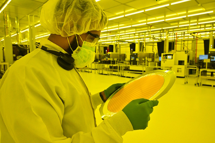
Now that you know how a wafer is turned into individual dies let’s talk about my first day in Malaysia and tie all the ends. On the first day of the Intel Technology Tour 2023, we visited the Penang Assembly and Test (PG16) facility. This is the place where high-volume chip manufacturing happens, and I was required to wear a “bunny suit” with additional protective gear (see photo below). We need to wear this protective gear as the assembly line is a dust-proof space. Furthermore, Intel did not even allow us to carry electronic items into PG16.


Bunny suits aside, this second half of the chip manufacturing process includes six key stages – attaching individual dies to the PCB, epoxy underfill, attaching the heat spreader, and, well, further testing. But we have condensed them into four major steps. Let’s look at how the Penang facility operates:
Step 3: Chip Attach
Remember the tape reels that we get from the Kulim facility, they are separated and attached to a PCB substrate (the green circuit board) alongside other components to give us the basic layout of the processor. Furthermore, for those wondering, Intel is now using a new and advanced 3D Foveros packaging technology, first introduced back in 2019, to stack individual dies in its latest processors.
But how does Intel mount the dies to the substrate? Well, this is where the next step in the process comes in. You see there’s a yellowish outline around the chip in the image below; it’s epoxy underfill that’s applied evenly to remove any gaps between the chips and the substrate.

This is also the step where the edges of the Meteor Lake (or other mobile chips) are lined with adhesive to attach the support bracket. The bracket is used to, as the name suggests, to give support and weight to the substrate that’s becoming thinner with each iteration. Intel doesn’t want the substrate to crack or chip under pressure, hence, the bracket is essential in newer chips.
Step 4: Lid Attach
Yeah, our processor is almost ready. Next up, a robot is seen applying thermal paste as well as adhesive on the processor to attach the lid or the Integrated Heat Spreader on top. While I didn’t get to see the process for a mobile chip, the GIF demonstrates the lid attach step on the Ponte Vecchio GPUs.


And voila! Your Intel processor is now ready for use, but before releasing it to the consumers, the company rigorously tests the chips for defects or anomalies.
Step 5: Burn-in & Testing
The completed CPU is loaded into trays and sent for electrical and stress testing. In this stage, Intel subjects its chips to extreme voltages and temperatures to ensure that only functional chips make it into the hands of the consumers. The stress tests are performed in Intel’s Penang facility in the Design and Development lab. As shown in the image below, this lab is packed with different equipment and a row of test benches to stress the CPU.


To wrap up, as part of the Intel Tech Tour Malaysia 2023, my trip to Intel Penang and Kulim facilities was fascinating. As consumers, we don’t really get to see the ins and outs of how each chip is made, why and how certain things are implemented, or how rigorous the testing is. But, thanks to Intel opening its doors to me and other global media personnel, giving us a chance to experience the magic and share it with our readers. So, did you find the chip-making and assembly process intriguing? Share your thoughts in the comments below.


